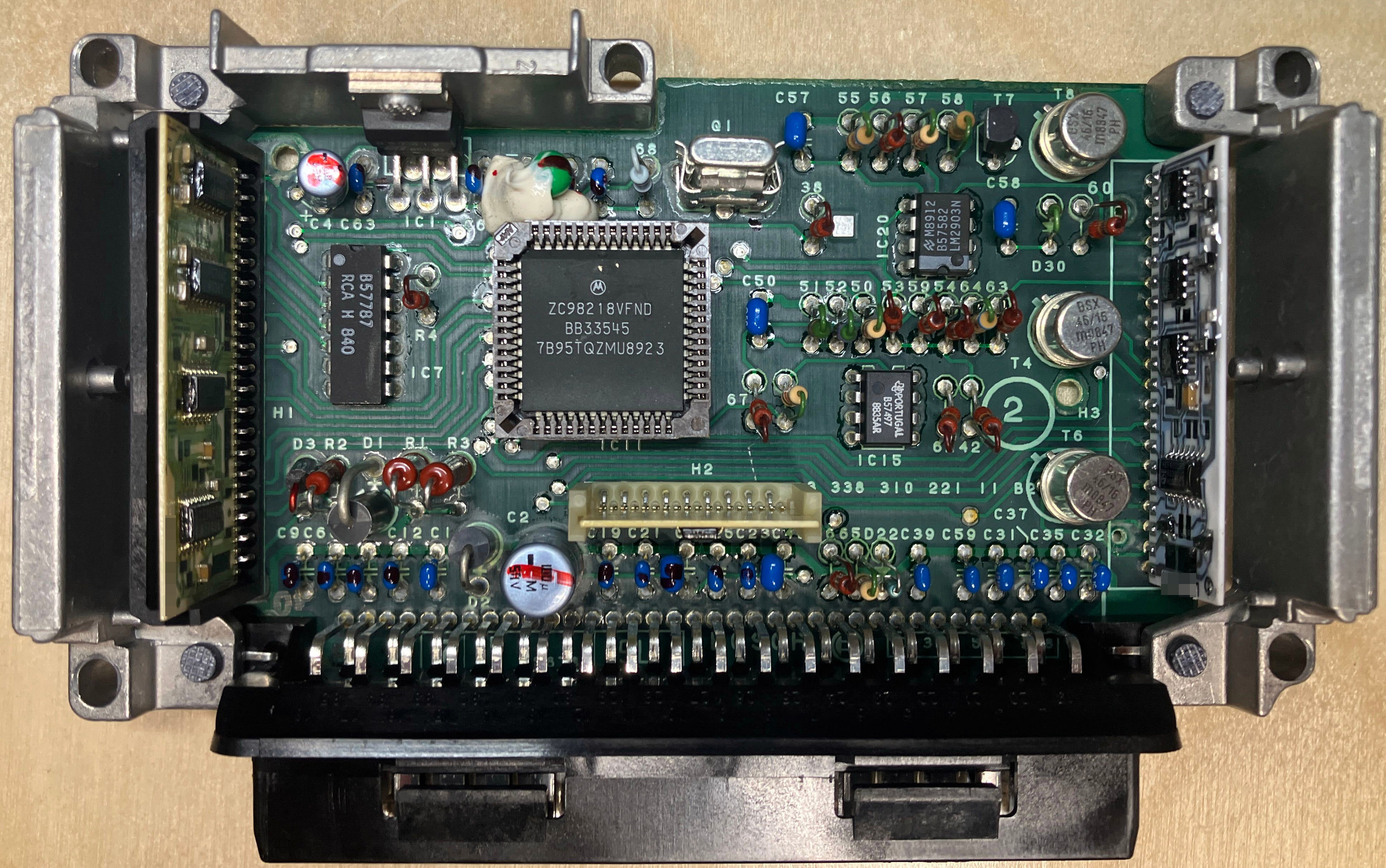
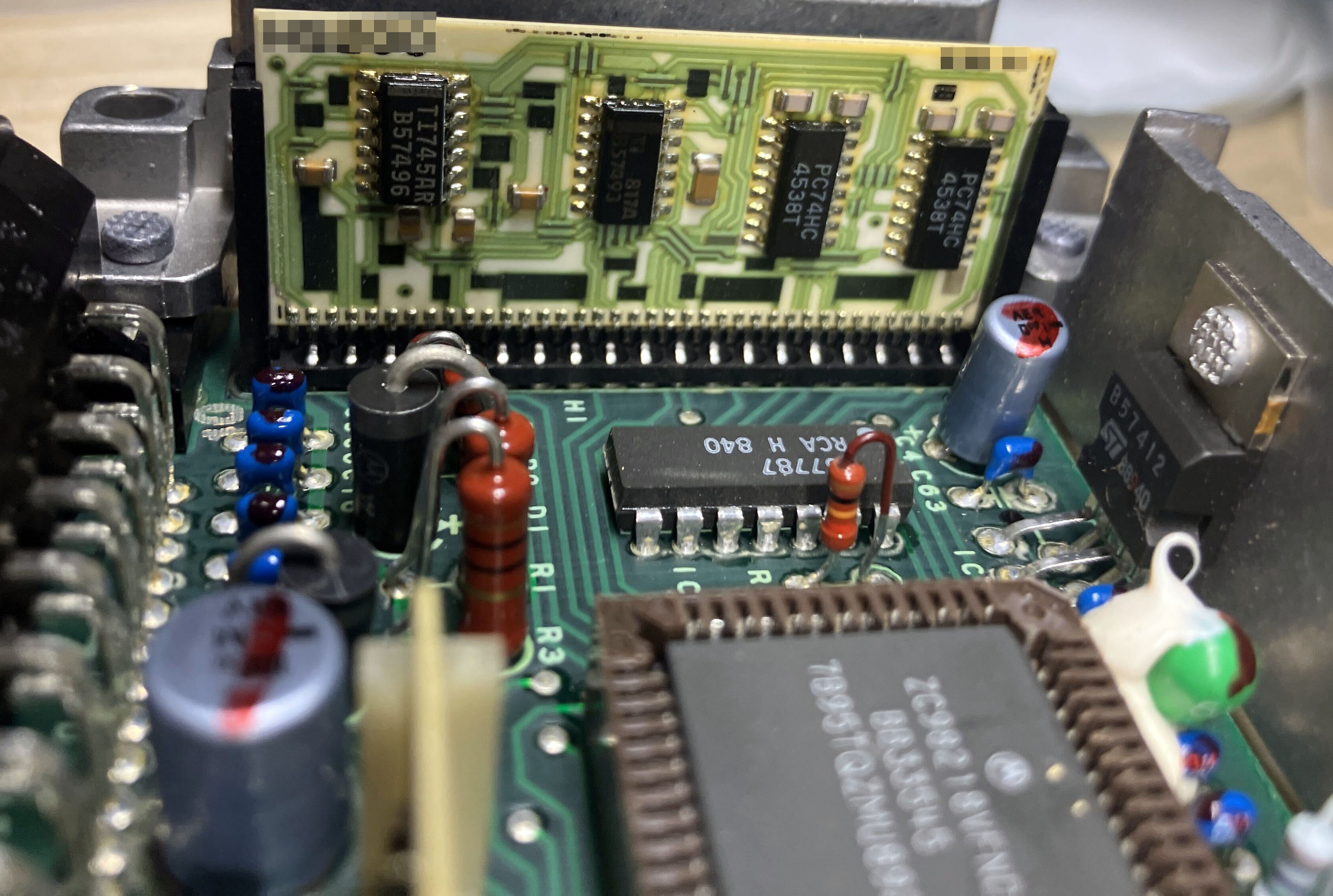
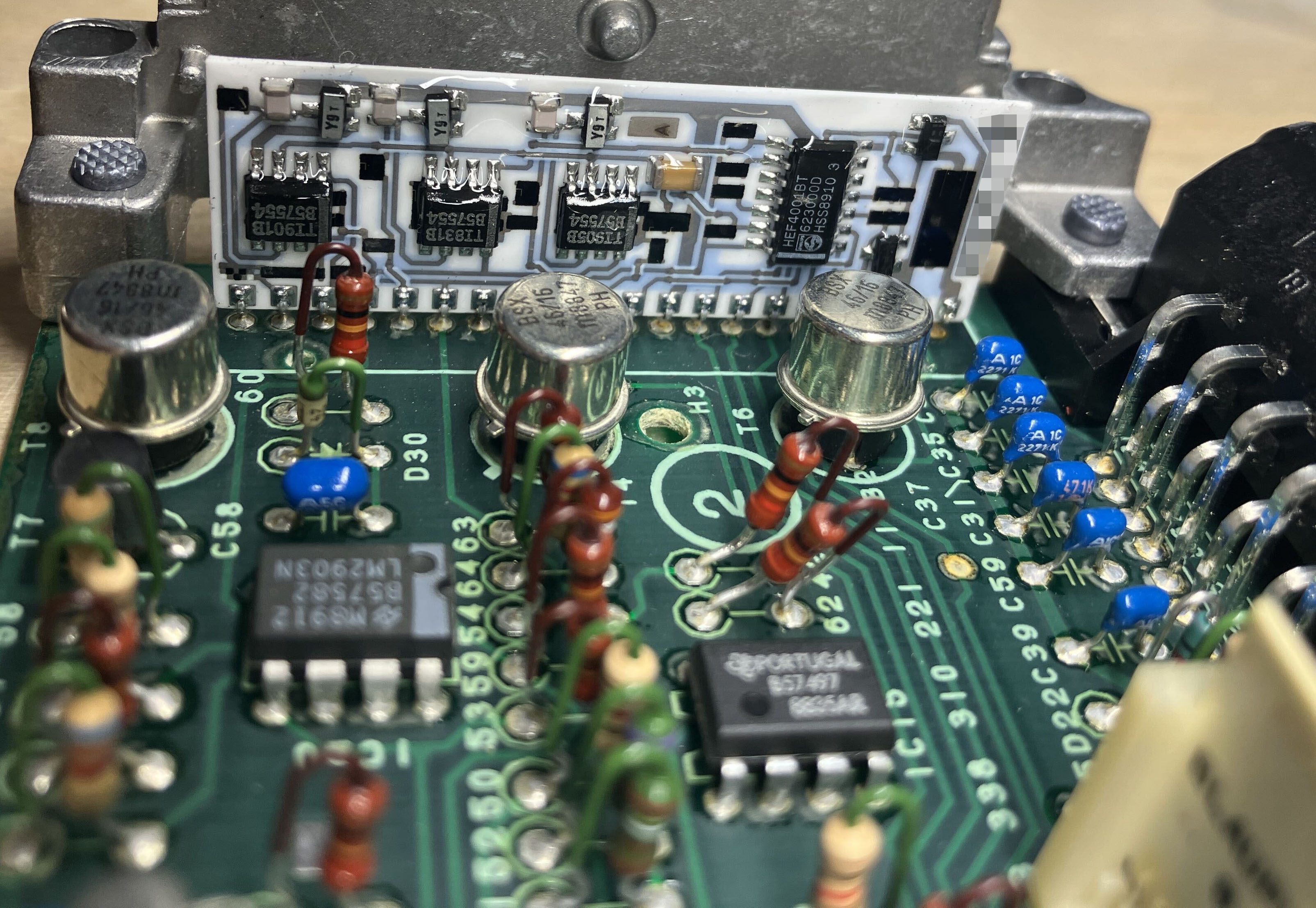
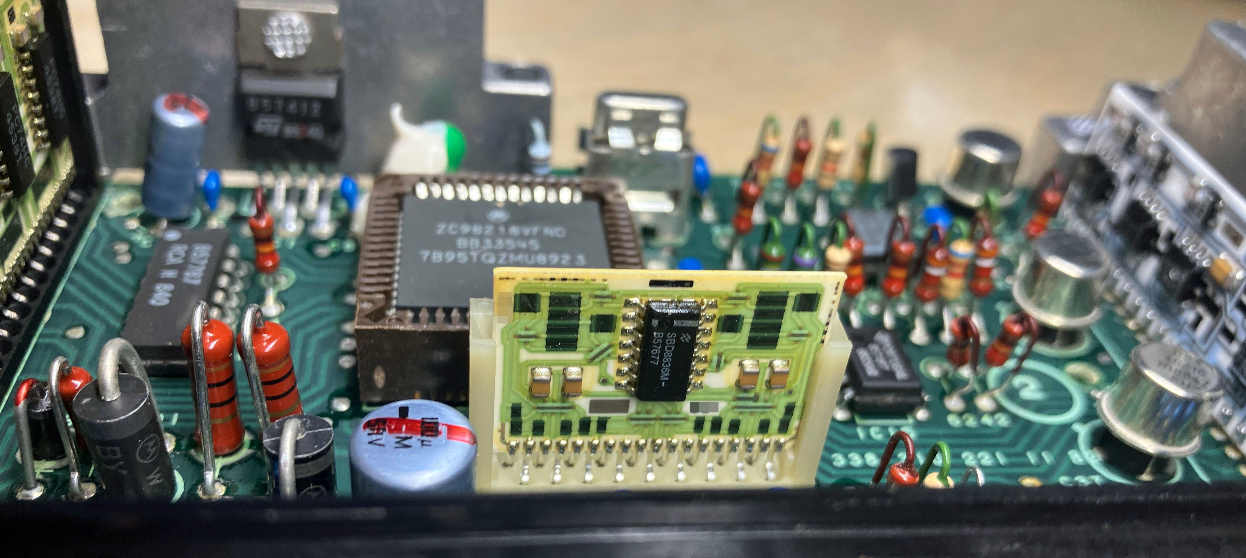
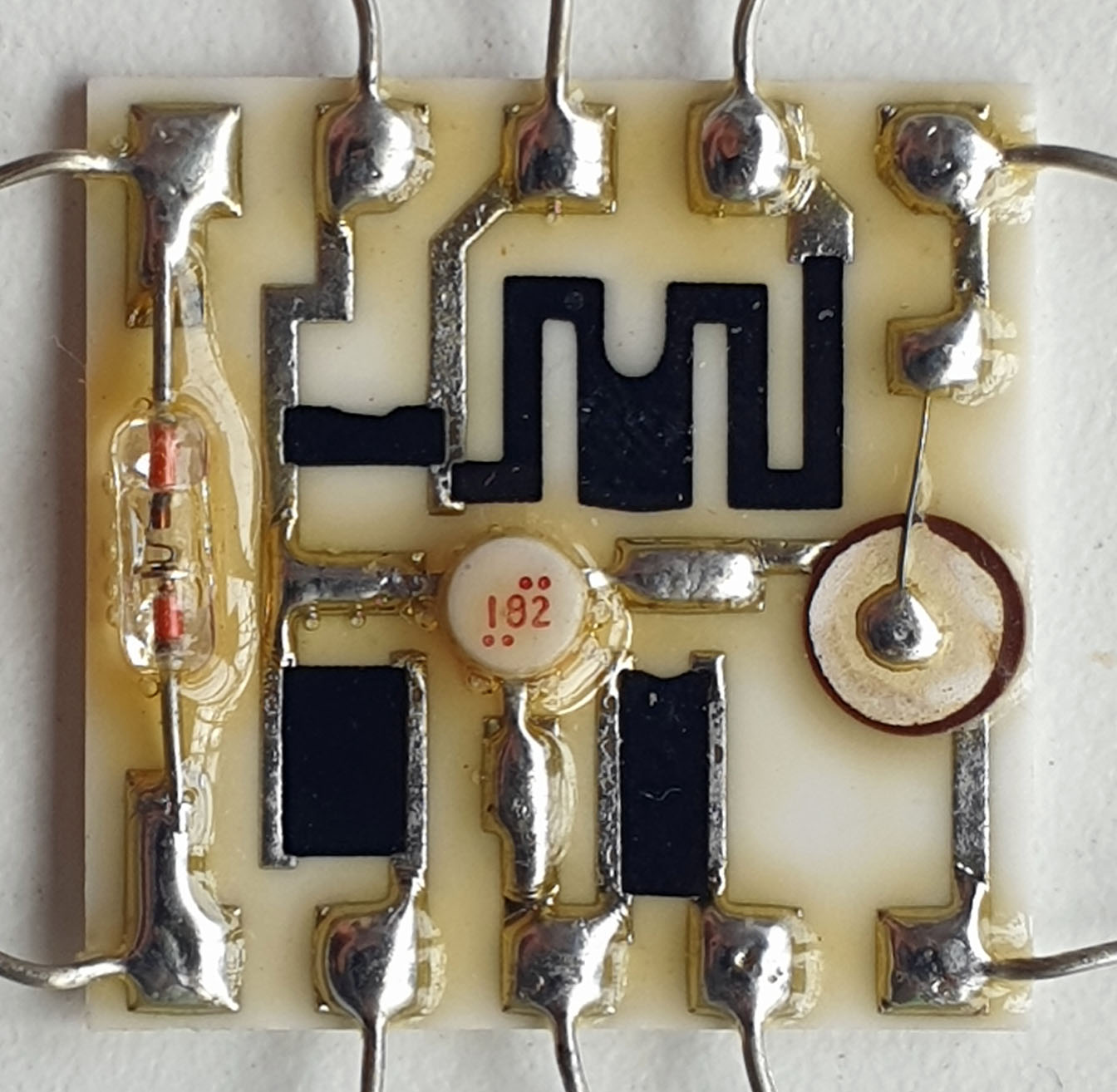
We seem to be on a theme of hybrid circuits! This aesthetically pleasing ware was submitted anonymously. Thank you, you know who you are!
While I realize that color palettes are not actually a deciding factor in most circuit board designs, I still appreciate it when things work out to have a nice color scheme overall. I like how the bold colors of the main circuit board draw contrast with the pastel earth-tones of the hybrid circuits.
The Ware for August 2026 is the “IC unit” from a Lafayette 150-in-1 “IC Electronic Project Kit”, part number 99-35107.
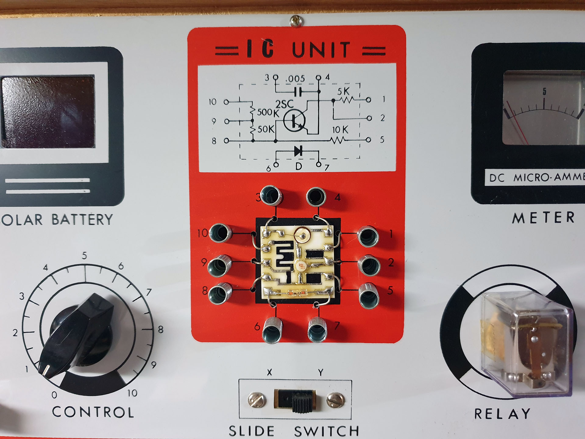
Above is a contextual photo of how the unit looked mounted in the kit.
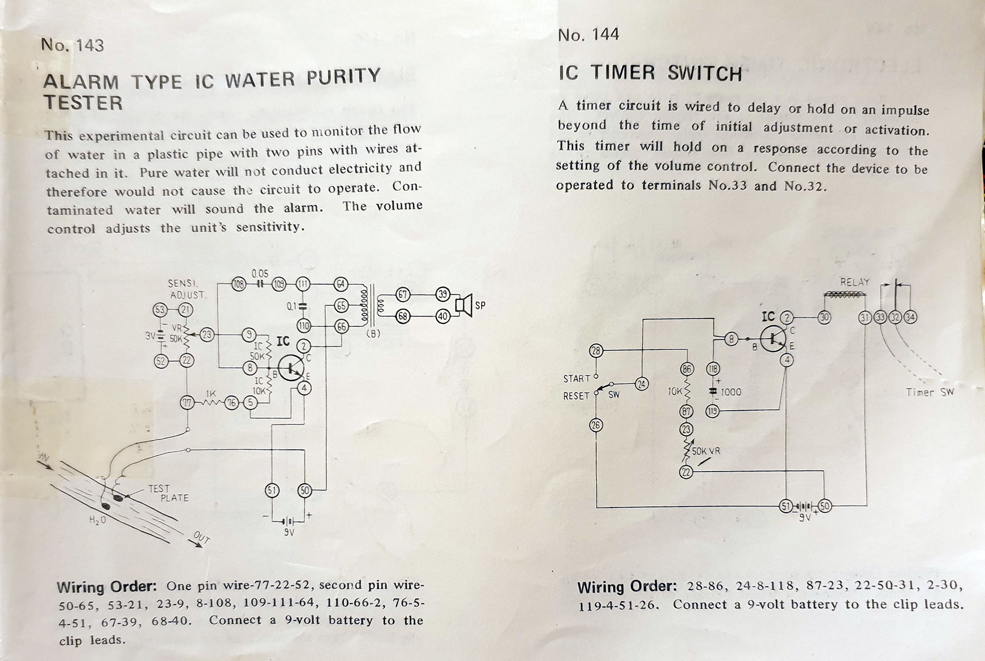
And above are a couple examples of projects you can build with the “IC” as part of the kit.
Answering Hales’ question, the part itself is covered with a clear overcoat of polymer that looks liquidy, but it is in fact a durable, hard coating. As a child, I appreciated how almost every part was out there and easy to see – you can really see the parallel-plate construction and dielectric of the capacitor, and if you look closely enough you can see the contact junction of the diode. It stimulated a sense of wonder and curiosity about how this all worked.
I’ll give the prize to Parkview! The IC module was re-used between a few generations of kits, so the 100-in-1 science kit is close enough for a guess. Congrats, email me for your prize.
The structure in question for last month’s ware are a pair of NPN transistors that form the core of a bandgap voltage reference circuit.
As its name implies, a bandgap voltage reference generates a near-constant voltage for use inside chips. The voltage is intended to be fairly constant over process variations, temperature variations, and power supply fluctuations. The circuit itself is extremely clever, using circuit elements that have offsets that move in opposite directions with temperature to cancel each other out. Without this circuit, chips would have performance characteristics that strongly depend upon its operating temperature. Therefore, almost every system on chip has at least one of these.
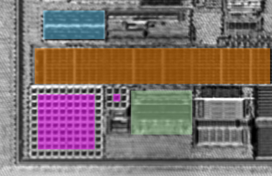
If you’re ever looking at a chip micrograph, the circuit will jump out because it’s likely to be the only thing that has two arrays of perfectly square NPN transistors next to each other. I’ve highlighted the active transistors in pink. In this case, the transistor ratio is 1:64. Modern chip designs will always include a ring of extra “dummy” transistors around the active transistors. The reason for the dummies is that they protect the core from process variations. At these insanely small geometries, a well-known problem is that transistors on the edge of an array behave differently from those in the core. This is due to a myriad of problems, but a simple example of the problem for visualization purposes is to imagine the devices going through an etching process: the concentration of the etchant will depend upon the density of the pattern being etched. The devices on the edge of an array will etch at a different rate than those in the center, and thus they will have a slightly different net performance characteristic. As a result, for very sensitive circuits like a bandgap voltage reference, it’s standard practice to “throw away” the edge devices as their characteristics are harder to control.
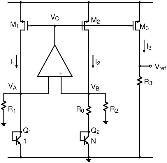
The orange region above the pair of NPN transistors is a pair of PMOS devices that are current mirrors that drive the NPN transistors. The blue square are a pair of resistors, and the green square is a differential amplifier that forms the active circuit core of the bandgap circuit. These circuits are so commonplace that it’s fairly easy to find a representative schematic just Googling for one:
The above was one of the first hits I got googling for “bandgap circuit“. The actual topology of this schematic is not exactly the same, but very similar to the circuit in the layout above.
When looking at a large, unknown die shot, I will often orient myself by first looking for a bandgap circuit, and then looking for an SRAM. Between the two of these, I get a size standard to which I can use to compare analog and digital circuits against, and work my way from there towards other functional elements on a chip.
While nobody guessed this circuit, asdf’s response gave me a chuckle, so I’ll give asdf the prize. Drop me an email to claim your prize!
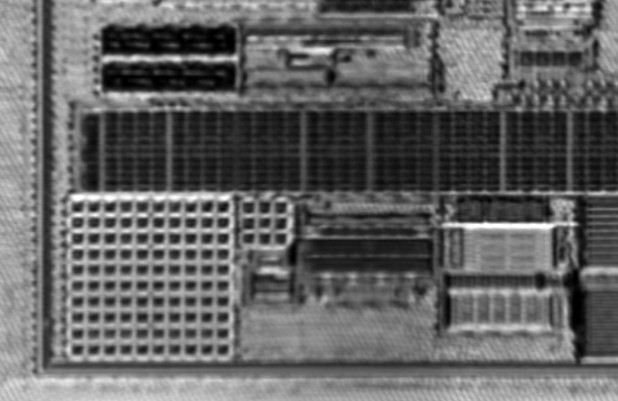
I’ve got silicon on the brain, so I’m going to give a die shot another go at name that ware. Hopefully this one is a bit easier than the last one. This excerpt is a design pattern I look for and find on almost every SoC. It’s technically showing a bit more than just the part I’m focused on, so as a hint I’m primarily interested in identifying the structure towards the lower left corner of this image.
If you’ve seen one of these before, you’ll know what it is – it’s pretty unmistakable, and a design pattern that’s highly conserved across processes, nodes and foundries. Bonus points to anyone that can explain some of the reasons why things are organized the way they are!